The Union Cabinet approved two more semiconductor projects under the India Semiconductor Mission on May 5, 2026. The projects include India's first commercial Mini/Micro-LED display facility based on Gallium Nitride technology and a semiconductor packaging facility. Both are planned in Gujarat, with a cumulative investment of about Rs 3,936 crore and expected employment for 2,230 skilled professionals.
The significance is not only that two more units were approved. It is that the approved mix points to a broader understanding of the semiconductor ecosystem. A chip economy is not just about advanced logic fabs. It includes compound semiconductors, sensors, display technologies, assembly, testing, marking, packaging, design tools, supply chains, workforce training, and reliable utilities. Countries that focus only on one layer usually discover that the rest of the value chain still sits elsewhere.
The Mini/Micro-LED project is especially interesting because display manufacturing is closely tied to consumer electronics, automotive screens, industrial equipment, augmented reality devices, and public digital infrastructure. Gallium Nitride-based display technology can support bright, efficient, high-performance modules. If India can build capability here, it may reduce dependence on imported display modules over time and create opportunities for domestic electronics brands.
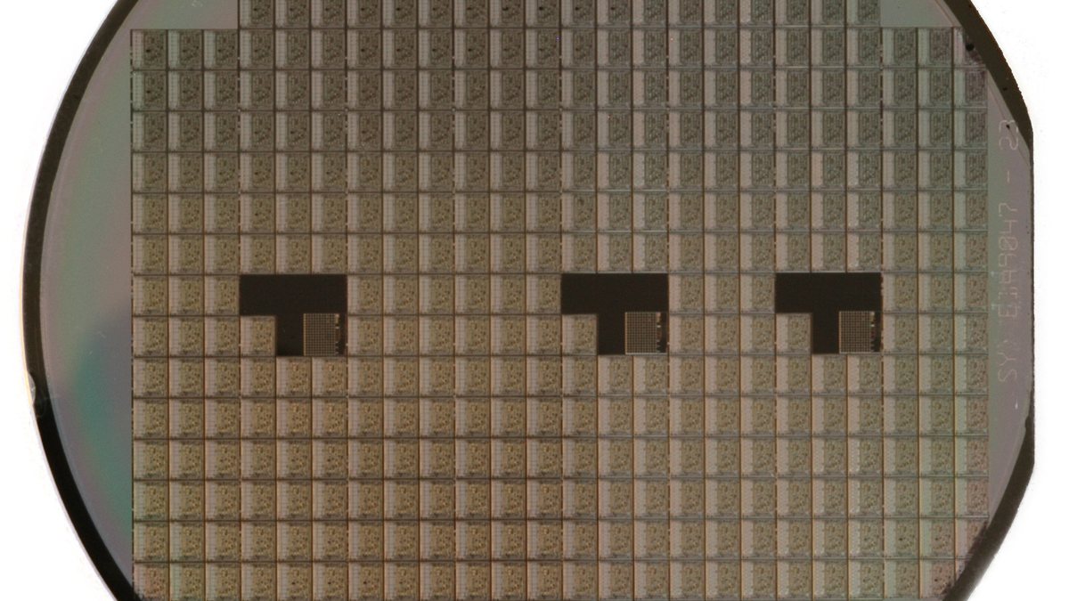
Packaging is the other quiet but critical layer. Advanced packaging decides how chips are connected, protected, tested, and made usable inside devices. Even when a wafer is fabricated elsewhere, packaging capability can capture value, create skilled jobs, and support local design companies. It also allows India to participate in semiconductor supply chains before every part of fabrication is localised.
The Cabinet release notes that India already has approved projects in various stages of execution, with two projects having started commercial shipments and two more expected to begin shipments soon. That detail matters because the semiconductor industry is judged by delivery, not intent. Investors, customers, and equipment suppliers watch whether timelines are met, whether quality is consistent, and whether local talent can scale.
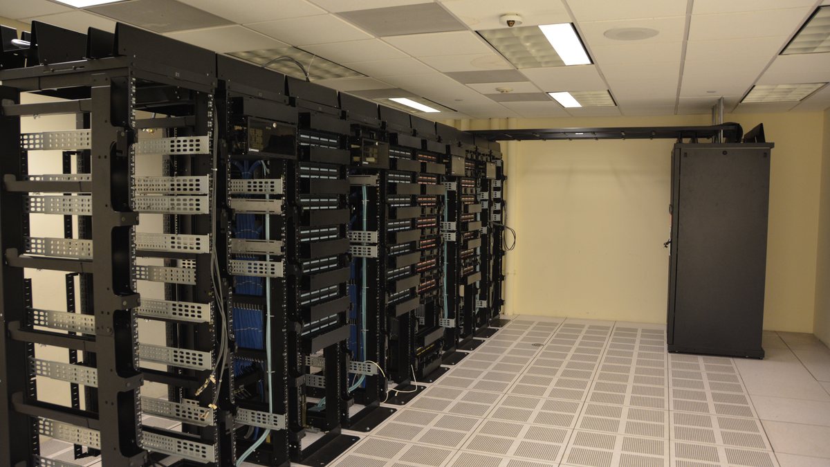
The policy challenge now is coordination. Semiconductor units need clean power, water management, specialty gases, chemicals, logistics, testing infrastructure, and fast customs processes. They also need universities and skilling institutions to produce technicians, process engineers, reliability experts, and equipment maintenance teams. The strongest chip clusters in the world are ecosystems, not isolated buildings.
For Gujarat, the approvals deepen its role as a manufacturing hub. For India, the larger value is strategic resilience. Semiconductors sit inside phones, cars, defence systems, medical equipment, power grids, telecom networks, and AI infrastructure. Supply disruptions can ripple through the whole economy. Building domestic capacity is therefore both an industrial policy and a national capability project.
The May 2026 approvals are a useful step in that direction. The next milestone will be visible production, reliable customer contracts, and a supplier base that grows around these units rather than remaining dependent on imports for every specialised input.
Sources Checked
These links were used for fact checking and context. The article above is original analysis and summary.